Product Description
RF-BM-ND02C is an RF module based on Nordic BLE SoC nRF51802QFAA with ARM? Cortex?-M0 32-bit processor. It integrates a 16 MHz crystal, an LC filter, an antenna matching and a meander line inverted-F PCB antenna. It features low power consumption, compact size, robust connection distance, and rigid reliability. It supports BLE stack v4.2 and can be preprogrammed with a serial interface communication protocol for simple programming. 1.27-mm pitch stamp stick package for easy assembling and cost-effective PCB design. RF-BM-ND02C is pin-to-pin compatible with RF-BM-ND02.
Parameters of RF-BM-ND02C
Chipset | nRF51802QFAA |
Supply Power Voltage | 1.8 V ~ 3.6 V, recommended to 3.3 V |
Frequency | 2402 MHz ~ 2480 MHz |
Transmit Power | -20.0 dBm ~ +4.0 dBm (typical: 0 dBm) |
Receiving Sensitivity | -93 dBm |
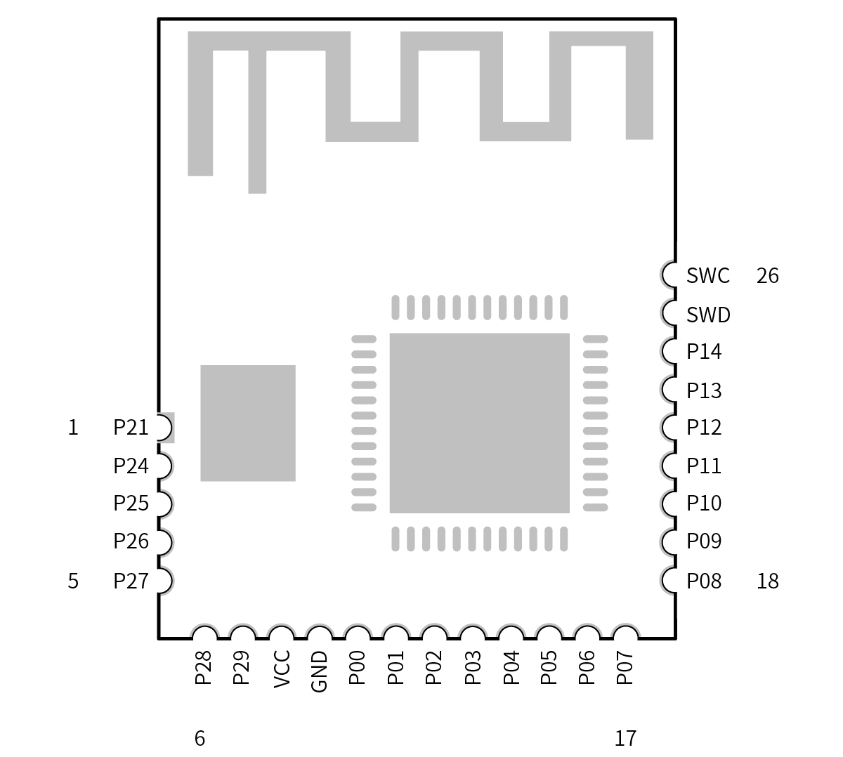
GPIO | 22 |
Crystal | 16 MHz |
RAM | 16 KB |
Flash | 256 KB |
Package | SMT Packaging |
Frequency Error | ±20 kHz |
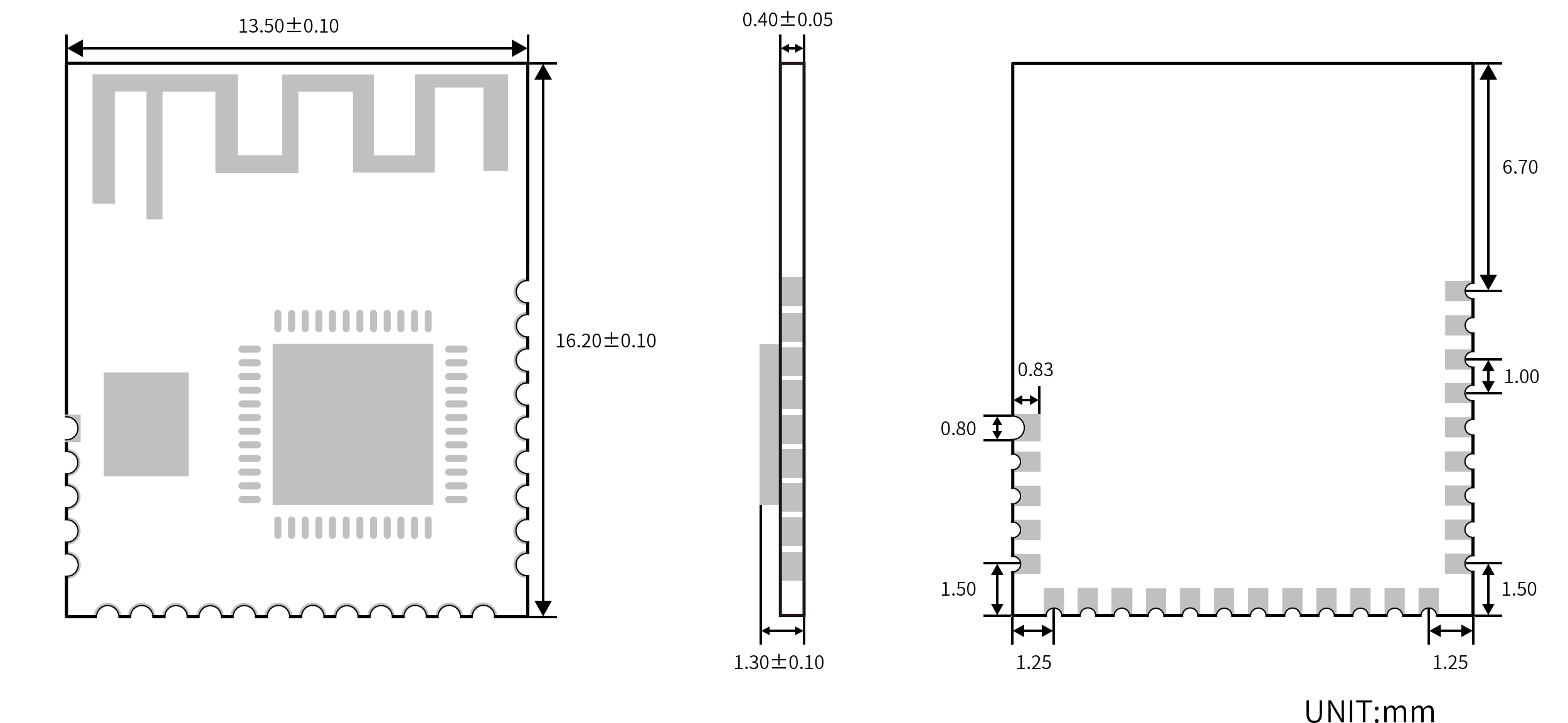
Dimension | 16.2 mm x 13.5 mm x (1.3 ± 0.1) mm |
Type of Antenna | PCB Antenna |
Operating Temperature | -20 ℃~ +70 ℃ |
Storage Temperature | -40 ℃~ +85 ℃ |